
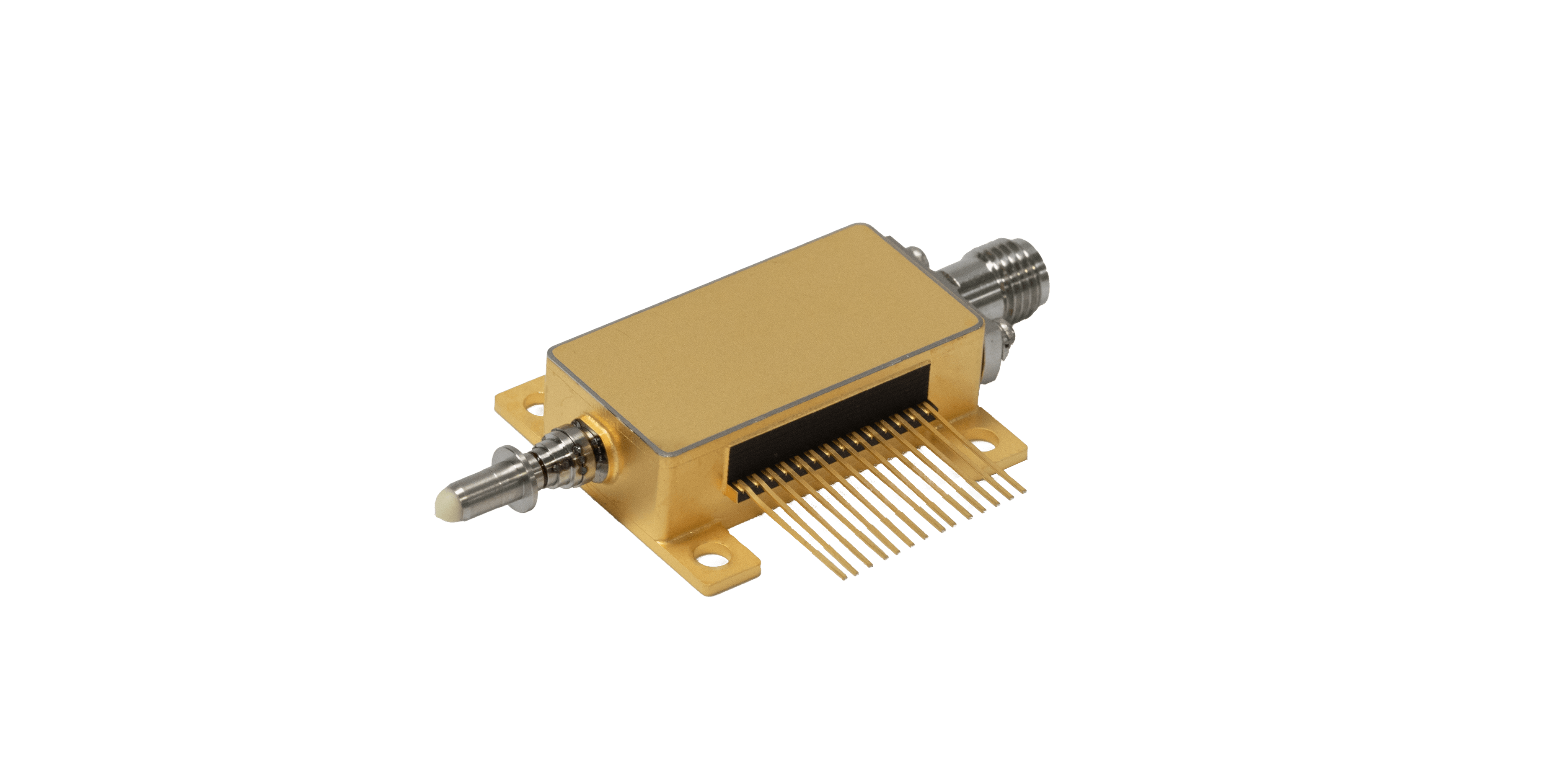
Compact optical design is often described as a footprint problem, but the real challenge is functional density. They reduce size when optical, electrical, thermal, and control interfaces are combined intelligently without sacrificing access or stability. Simply choosing a small component can move complexity into cables, bias circuits, alignment fixtures, or cooling structures elsewhere in the product.
Within compact assemblies, thin-film lithium niobate supports waveguides and electrodes that can deliver high-speed modulation in relatively small structures. Packaged products may integrate fiber coupling, RF connectors, and even a light source.
Each integration choice changes who owns alignment, laser selection, repair, calibration, and qualification, so compactness must be evaluated across the complete assembly lifecycle. They compare the packaged assembly against a discrete baseline using identical driver and optical conditions, which prevents size claims from being separated from power or loss penalties.
Across TFLN Devices, available functions include intensity, phase, IQ, integrated-source, and frequency-comb products across several bandwidths. They examine how these options can simplify optical engines and instruments, while requiring evidence that insertion loss, drive voltage, thermal behavior, connector access, and long-term stability remain acceptable in the reduced mechanical envelope.
Compactness Comes from Removing Interfaces, Not Merely Shrinking Parts
Compact optical modulators can shorten RF and fiber paths, reducing cable loss, reflection, and alignment points. Those gains are useful when connectors and mounting remain practical.
They model bend radius, strain relief, heat flow, board keep-outs, and service access before assigning a component footprint, because the surrounding mechanical volume often exceeds the package outline. From the driver perspective, TFLN devices may reduce the required driver swing through practical half-wave voltage while preserving bandwidth.
This can reduce amplifier size or power, but a smaller thermal solution is justified after they measure large-signal operation and temperature rise. They calculate total heat from driver, laser, bias control, and nearby electronics, not just the passive optical package. Optical integration also affects loss.
Combining functions can remove external connectors or couplers, yet internal waveguides, splitters, and alignment still consume power. They request reference-plane definitions and loss breakdowns, then create a complete optical budget. A compact design that requires a larger laser or amplifier may not improve system size or energy.
Different Modulation Functions Need Different Packaging Choices
Optical intensity modulators support direct-detection links and pulse control with comparatively simple optical paths. Listed 40 GHz and 67/110 GHz versions provide different size and performance options. They compare connector orientation, bias interface, package dimensions, and cable requirements alongside bandwidth, insertion loss, and half-wave voltage when fitting them into an optical engine.
For phase and IQ functions, TFLN devices include more complex routing or controls. A phase unit may serve sensing and microwave photonics, while an IQ package supports coherent QPSK or QAM. The integrated function can eliminate external interferometers, but it adds bias points and calibration needs.
Mechanical compactness must be accompanied by accessible control and monitoring. An intensity product with a built-in low-RIN source demonstrates another integration path. The listed 40 GHz bandwidth and 12 dBm on-state output can reduce separate laser packaging, yet source wavelength, replacement strategy, isolation, thermal coupling, and lifetime become part of the module decision.
They compare this route with a separate-laser architecture over expected production and service conditions. Cable exit direction and connector retention are tested during mechanical prototypes, because these details can determine whether the compact unit fits the final enclosure and assembly sequence.
A Smaller Assembly Must Still Be Manufacturable and Serviceable
During compact-product assembly, tolerance control governs the yield of TFLN devices. Small packages can demand precise fiber and RF placement, and limited access may make rework difficult. They review alignment methods, adhesive control, connector torque, mounting flatness, and incoming inspection.
Pilot builds reveal whether the mechanical concept is repeatable rather than merely possible with expert handling. Compact optical modulators also need test access. They plan wafer, package, and final-system measurements that can isolate loss, bandwidth, bias, and connector faults without disassembling the product. Integrated monitors or defined loopback modes may reduce diagnostic time.
Design-for-test is especially important when multiple functions share one package and a failure could otherwise remain ambiguous. Serviceability depends on the product class. A sealed instrument may replace an entire optical subassembly, while field-deployed communication equipment may need modular replacement and stored calibration.
They document serial tracking, firmware compatibility, spare policy, and recalibration steps. A reduced footprint should not create an opaque component that is difficult to support after launch. Volume cost models include rework and calibration time, not merely package price, so that functional density is evaluated through actual manufacturing effort.
Compact modulator design succeeds when integration removes meaningful interfaces and preserves the operating margin of the full product. Thin-film lithium niobate can contribute wide bandwidth and practical drive within smaller structures, but packaging, thermal control, optical loss, bias management, and test access determine whether the space saving is genuine.
They compare candidate assemblies through mechanical models, optical and electrical budgets, thermal measurements, pilot production, and service scenarios. These activities often reveal that a compact package is not necessarily a low-risk architecture.
The selected design balances size with yield, diagnosability, supplier responsibility, and stable performance over the intended environment. A compact modulator still needs workable connector access, thermal paths, driver behavior, and assembly yield. Mechanical and electrical layouts using Liobate packages can reveal whether the density gain remains practical to build and maintain.